Dismantling The Card
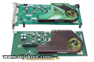
We first dismantled the card to take a look at the second PCB and see how much it differs from the first PCB. Let's take a look!
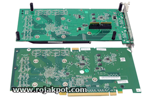
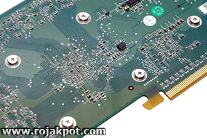
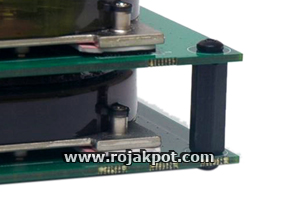 The two PCBs are separated by hexagonal spacers placed at the four corners of the card. The spacers not only ensures a fixed space between the two PCBs, it also provides support for this rather unwieldy card.
The spacers are secured to the PCBs by a screw on both ends. Because one of the screws also secures the back plate, the screws on the back PCB should be unscrewed first. This allows you to detach the back PCB from the front PCB.
As you can see, the two PCBs look very similar to each other. They are the same length and have the same cooler. But there are quite a few differences.
For starters, front PCB is host to the card's dual DVI and HDTV outputs as well as its PCI Express power connector. The SLI and PCI Express connectors are on the back PCB. The back PCB also appears to have a few extra surface-mounted components, including a bridge chip hidden under the cooler.
Removing The Cooler
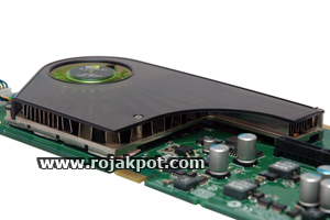
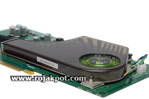
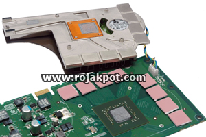
We then proceeded to remove the cooler to have a look under it. That would also allow us to closely inspect the fan and heatsink design. We used the back PCB as our example here. As you can see in these pictures, the cooler is a little bigger than what was used in the GeForce 7900 GT and GeForce 7600 GT.
Removing the cooler wasn't very difficult. In fact, there were only five screws to remove and voilà! the cooler popped off!
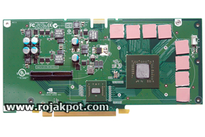
The card is populated mainly by the GeForce 7950 GX2 GPU, eight GDDR3 memory chips and a PCIe switch chip. The front PCB should look about the same, minus the switch chip.
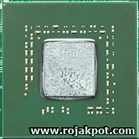
The GPU and the PCIe switch chip are covered in thermal paste while the memory chips are covered with thermal tapes. Note the white line going around the area. That actually corresponds to the outline of the cooler.
The GPU doesn't look like much, all smudged up in thermal paste, but that's the spanking new GeForce 7950 GX2 right there.
<<< The Exhaust Vents And Power Connector, The PCI Express And SLI Connectors : Previous Page | Next Page : The Cooler >>>


 Add to Reddit

