AMD Carrizo APU Details Revealed!
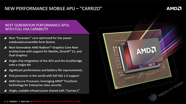
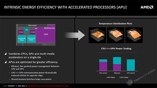
February 23, 2015 — AMD (NASDAQ:AMD) revealed at the prestigious International Solid State Circuits Conference (ISSCC) that the upcoming A-Series Accelerated Processing Unit (APU), codenamed “Carrizo”, for notebooks and low-power desktops will deliver a wealth of new, advanced power management technologies while achieving substantial performance through new “Excavator” x86 CPU cores and a new generation of AMD Radeon™ GPU cores. Using a true System-on-Chip (SoC) design, AMD expects Carrizo to reduce the power consumed by the x86 cores alone by 40 percent, while also providing substantial gains in CPU, graphics, and multimedia performance over the prior generation APU.
“As a part of our continued focus on building great products, the advanced power and performance optimizations we have designed into our upcoming ‘Carrizo’ APU will deliver the largest generational performance-per-watt gain ever for a mainstream AMD APU,” said Sam Naffziger, AMD Corporate Fellow and co-author of the AMD presentation at ISSCC.
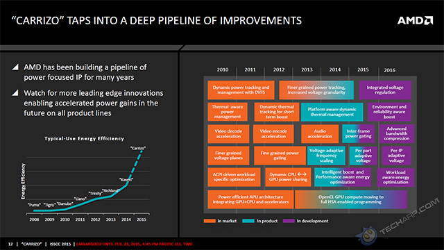
“There have been remarkable advances in performance and energy efficiency in computing since the birth of the modern microprocessor. However, the energy-related benefits that flow from new manufacturing processes have slowed, ushering in an era when alternative ways to improve processor performance and efficiency are needed. AMD has been pursuing Heterogeneous System Architecture (HSA) and proprietary power management technologies to make continued gains. The upcoming ’Carrizo’ APU takes a big step toward the AMD 25x20 energy efficiency goal and incorporates a wealth of new features that will be adopted across our full product line going forward.”
The Tech ARP 2015 Mega Giveaway Contest
| If you like this article, please share it! -> |
New Carrizo Disclosures at ISSCC
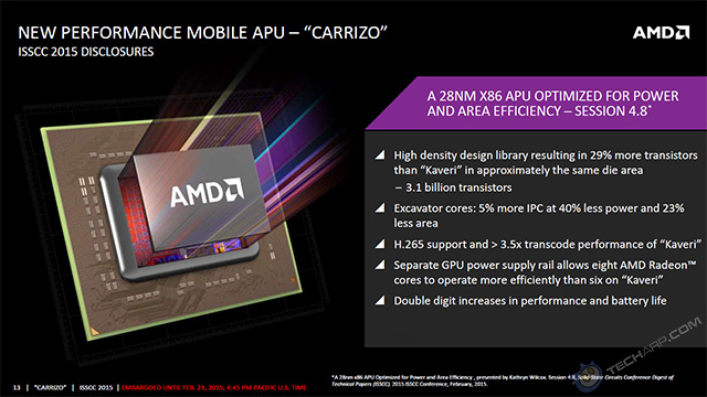
- 29% more transistors in nearly the same die size as its predecessor, “Kaveri”;
- New “Excavator” x86 cores provide an uplift in instructions-per-clock at 40% less power;
- New Radeon GPU cores with dedicated power supply;
- Dedicated, on-chip H.265 video decode;
- Double digit percentage increases in both performance and battery life;
- Integrated Southbridge for the first time on an AMD high-performance APU.
Details will be presented at the AMD ISSCC session, “A 28nm x86 APU Optimized for Power and Area Efficiency,” by AMD Fellow and Design Engineer Kathy Wilcox. The presentation covers the technology, implementation, and power management features of the Carrizo APU.
| If you like this article, please share it! -> |
Architectural Advances
New high density design libraries allowed AMD to fit 29 percent more transistors on Carrizo – 3.1 billion – in nearly the same chip size as the previous generation, Kaveri APU. This density increase has allowed a larger area for graphics, multimedia offload, and integration of the “Southbridge” system controller on a single-chip. The increased support for multimedia includes the new, high-performance H.265 video standard and double the video compression engines of its predecessor.
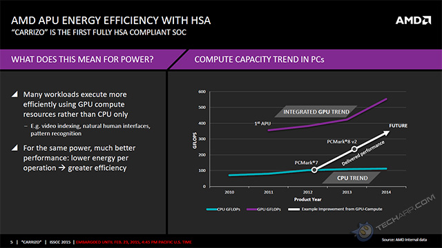
The inclusion of H.265 in hardware will support true 4K resolutions, help extend battery life, and reduce bandwidth requirements when viewing compatible video streams. The additional transistor budget also allows Carrizo to become the first processor in the industry designed to be compliant with the HSA 1.0 specification developed by the HSA Foundation. HSA makes programming accelerators such as the GPU far simpler, ideally leading to greater application performance at low power consumption.
Chief among the design advantages for HSA is the heterogeneous Unified Memory Access (hUMA) within Carrizo. With hUMA, the CPU and GPU share the same memory address space. Both can access all the platform’s memory and allocate data to any location in the system’s memory space. This coherent-memory architecture greatly reduces the number of instructions required to complete many tasks, thus helping improve both performance and energy efficiency.
| If you like this article, please share it! -> |
Support Tech ARP!
If you like our work, you can help support out work by visiting our sponsors, participate in the Tech ARP Forums, or even donate to our fund. Any help you can render is greatly appreciated!
Page |
AMD Carrizo Details Revealed! |
1 |
• AMD Carrizo Press Release |
2 |
Support us by buying from Amazon.com! |
|
| Grab a FREE 30-day trial of Amazon Prime for free shipping, instant access to 40,000 movies and TV episodes and the Kindle Owners' Lending Library! | |


 Add to Reddit

