The ASUS EN7900GS TOP
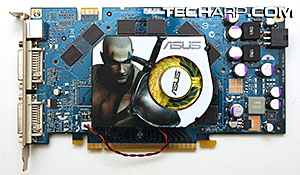
The EN7300GS TOP looks just like the NVIDIA GeForce 7900 GT reference card, from the PCB down to the cooler. Unlike what the box promised, the sticker on the cooler shroud sports a more macho warrior. I wonder what happened to that cute warrior chick. ![]()
Jokes aside, the card looks and feels exactly like a GeForce 7900 GT. No reason why it should not. After all, the only difference between the two cards is the number of pixel and vertex shaders in the GPU itself. The GeForce 7900 GT has 24 pixel shaders and 8 vertex shaders, while the GeForce 7900 GS only has 20 pixel shaders and 7 vertex shaders. Otherwise, both cards are identical.
However, you should note that while both GeForce 7900 GT and GeForce 7900 GS run at 450MHz, ASUS overclocked the GPU in the EN7900GS TOP to 590MHz. That's 31% higher than the rated clock speed. In fact, it gives the EN7900GS TOP a much higher fill rate than the NVIDIA GeForce 7900 GT!
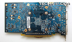
All eight GDDR3 memory chips were arrayed in pairs around the cooler. For certain, none of them are directly cooled by the cooler. The back is totally clear of significant components. But you can see the four screws used to hold the cooler in place.
Specifications
Here are the specifications of the ASUS EN7900GS TOP. Do note that these are not the specifications for the regular NVIDIA GeForce 7900 GS card.
Manufacturing Process |
• 0.09 Micron |
Transistor Count |
• 278 Million |
DirectX Support |
• 9.0c |
Interface |
• PCI Express |
Vertex Shaders |
• 7 |
Vertex Shader Version |
• 3.0 |
Pixel Shaders |
• 20 |
Pixel Shader Version |
• 3.0 |
Textures Per Clock |
• 20 |
ROPs |
• 16 |
Core Speed |
• 590 MHz |
Fill Rate |
• 11800 MTexels/s |
Memory Bus Width |
• 256 -bits |
Memory Size |
• 256 MB |
Memory Type |
• GDDR3 |
Memory Speed |
• 720 MHz (1.44 GHz DDR) |
Memory Bandwidth |
• 46.08 GB/s |
DVI Support |
• Two dual-linked DVI, both integrated into the GPU |
Features |
• Microsoft®
DirectX® 9.0 Shader Model 3.0 Support |
Now, let's take a closer look at the card.


 Add to Reddit


