


 Add to Reddit

The NVIDIA GTX 200 Series Is Out!
When the ATI Radeon HD 4850 was scheduled to be launched on June 18, NVIDIA decided to spoilt their party by scheduling the launch of their new GTX 200 series of graphics cards a day earlier. Then ATI decided not to play the game and delayed their launch to June 25.
Now that there was no reason to launch on June 17, NVIDIA apparently decided to speed up the launch, by one day to June 16. Well, today's the day NVIDIA officially launches their GTX 200 series of graphics card!
Although many of us have already read about and even seen photos of the two new NVIDIA GTX 280 and GTX 260 graphics cards, today is the day we can finally tell you the whole story about the two cards. Yes, we behaved like gentlemen and we kept to our NDAs, even though their spy really pissed us off. ![]()
Alright, now that everything's in the open now, let's get onto the good stuff - the new NVIDIA GT200 GPU and the two new NVIDIA GTX 280 and NVIDIA GTX 260 graphics cards. ![]()
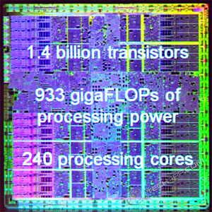
The NVIDIA GT200 GPU
 |
The nomenclature is a bit confusing, so forgive us if we do make any mistakes here. Both the GTX 280 and the GTX 260 are based on the NVIDIA GT200 GPU, although there are some who call it the GTX200. I guess it could be used interchangeably although it would be more accurate to call the GPU, GT200 and the card series, GTX 200.
In any case, the new NVIDIA GT200 has 240 stream processors (or processing cores), which generate about 933 gigaFLOPs of processing power. To achieve that requires a lot of transistors - an astounding total of 1.4 billion transistors.
This, plus the fact that it is still built on the 65 nm process technology, inevitably meant the GT200 would be a very large chip. With a die size of 575 mm2, it is approximately 5x the size of an Intel Core 2 Duo E8400 processor.
Unlike the G92, the GT200 is not based on the first-generation G80 architecture, but rather an improved second-generation unified architecture that includes amongst other things, twice the number of registers and fast local memory shared by stream processors within a cluster. Here are the key features of the new GT200 GPU :
- Second-generation unified architecture
- 240 processing cores
- Next-generation geometry shading and stream out performance
- Improved dual-issue
- Twice the number of registers
- New texture scheduler
- Highly scalar SIMT (single instruction, multiple task) design
- Local 16k shared memory (per cluster of 8 stream processors)
- Double precision accuracy
- 3x ROP blending performance
- Advanced compression technology turned for extreme HD resolutions
- Support for 3-way NVIDIA SLI technology
- Support for future 10-bit colour and 120 Hz LCD panels
While ATI is fond of using newer memory technologies like GDDR5 in the Radeon HD 4870, NVIDIA preferred to stick with the tried and true GDDR3 memory for the GTX 280 and GTX 260. Both the NVIDIA GTX 280 and the NVIDIA GTX 260 use the same GT200 GPU. They only differ in the number of stream processors enabled, the size of their memory bus width and the size of their memory buffer. Let's take a look at each of them...
Support Tech ARP!
If you like our work, you can help support out work by visiting our sponsors, participate in the Tech ARP Forums, or even donate to our fund. Any help you can render is greatly appreciated!
Page |
Topic |
||
1. |
|||
2. |
|||
3. |
|||
| |