Introduction
NVIDIA launched the GeForce GTX 280 and GTX 260 graphics cards on June 17, 2008. Both are based on the NVIDIA GT200 GPU which uses NVIDIA's improved, second-generation unified architecture. The new GT200 GPU, features amongst other things :
- 240 stream processors
- Twice the number of registers
- Fast local 16k shared memory (per cluster of 8 stream processors)
- New texture scheduler
- Double precision accuracy
- 3X ROP blending performance
For more information on the NVIDIA GT200 GPU, please take a look at the NVIDIA GTX 280 & GTX 260 Technology Report.
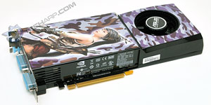
As one of NVIDIA's biggest retail partner, ASUS has no less than seven different GTX 280 models. They consist of three versions, each available with or without HDMI support. The three major versions are the basic ENGTX280, the ENGTX280/G game bundle kit and the top-of-the-line ENGTX280 TOP or OC overclocked edition. The card we are reviewing is the ASUS ENGTX280 TOP which ASUS says is 12% faster than "regular" GeForce GTX 280 cards.
Before we start with the actual review, let's take a look at how the ASUS ENGTX280 TOP compares against a few graphics cards, including the standard GeForce GTX 280.
|
ASUS ENGTX280 |
GeForce |
GeForce |
Radeon HD 4870 |
GeForce |
Architecture |
GT200 |
GT200 |
GT200 |
RV770 XT |
G92 |
Manufacturing |
65 nm |
65 nm |
65 nm |
55 nm |
55 nm |
Transistor |
1400 Million |
1400 Million |
1400 Million |
956 Million |
754 Million |
DirectX |
10 |
10 |
10 |
10.1 |
10 |
Interface |
PCIe 2.0 |
PCIe 2.0 |
PCIe 2.0 |
PCIe 2.0 |
PCIe 2.0 |
Stream Processors |
240 |
240 |
192 |
800 |
128 |
Textures Per Clock Cycle |
80 |
80 |
64 |
48 |
64 |
ROPs |
32 |
32 |
28 |
16 |
16 |
Vertex
Shader |
4.0 |
4.0 |
4.0 |
4.1 |
4.0 |
Pixel Shader |
4.0 |
4.0 |
4.0 |
4.1 |
4.0 |
Core Speed |
670 MHz |
602 MHz |
576 MHz |
750 MHz |
738 MHz |
Texture Fill Rate |
53,600 MTexels/s |
48,160 MTexels/s |
36,864 MTexels/s |
36,000 MTexels/s |
47,232 MTexels/s |
Pixel Fill Rate |
21,440 MPixels/s |
19,264 MPixels/s |
16,128 MPixels/s |
12,000 MPixels/s |
11,808 MPixels/s |
Memory
Bus |
512-bits |
512-bits |
448-bits |
256-bits |
256-bits |
Memory |
GDDR3 |
GDDR3 |
GDDR3 |
GDDR5 |
GDDR3 |
Memory Speed |
1215 MHz |
1107 MHz |
999 MHz |
900 MHz |
1100 MHz |
Memory |
155.52 GB/s |
141.67 GB/s |
111.89 GB/s |
115.20 GB/s |
70.40 GB/s |
Although the new GT200 GPU has 240 stream processors, it delivers only an average of 80 textures per clock cycle, just 25% more than what G92-based graphics cards (like the GeForce 9800 GTX+ and the GeForce 8800 GTS 512MB) are capable of. Because it runs at a much slower clock speed of 602 MHz, it actually has about the same texture fillrate as the GeForce 9800 GTX+. On the other hand, the GT200 has a much higher pixel fillrate with a very healthy boost in memory bandwidth to boot.
NVIDIA initially pegged the GeForce GTX 280 as far superior to the ATI Radeon HD 4870 (with a stratospheric price to match). Their specifications seem to show it too, but when the Radeon HD 4870 proved to be much faster in real life, beating even the much-vaunted GeForce GTX 260, NVIDIA had to take both the GTX 280 and GTX 260 down in price and position. The new price point, coupled with its support for PhysX, now makes the GeForce GTX 280 a much more attractive proposition than it initially was.
ASUS took the GTX 280 one step further, offering the factory-overclocked TOP or OC editions which they promise would deliver at least 12% better performance than the standard GeForce GTX 280. They did so by overclocking the core by 11.3% to 670 MHz and the GDDR3 memory by 9.8% to 1215 MHz. Will it be as fast as they claim it to be? We will see soon enough.
Support Tech ARP!
If you like our work, you can help support out work by visiting our sponsors, participate in the Tech ARP Forums, or even donate to our fund. Any help you can render is greatly appreciated!


 Add to Reddit

