


 Add to Reddit

The X800 Pro Ultra 2X (Continued)
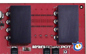
Lets have a closer look at that ram chip.

RAM Close Up
(pic big enough but too blur, pls retake it!)
ATI used something that looked like really sticky thermal tape to bind the
heatsink to the memory chips. Even after removing the heatsink, there was still
quite a lot of residue. Even alcohol had no effect on the residue. But they
look like the same GDDR3 chips used in standard X800 Pros (the boring single
VPU cards ![]() ).
There's are 16 memory chips with a total capacity of 512MB!
).
There's are 16 memory chips with a total capacity of 512MB! ![]()
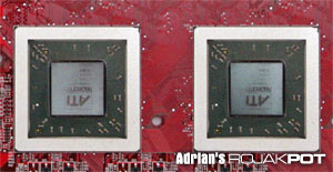
Here's a shot of the dual VPUs.
Dual VPUs
These are the dual VPUs. This is a good move I think as it allows the source
of heat to be concentrated on one portion of the card and the heatsink is designed
to remove a lot of heat (dual slot design.) Man, looking at it makes me drool...
![]()
Here's a shot of the four pin Molex connectors.
MOlex connectors
I dont really like the way the molex connectors are placed on the card. Its a bit too tight. It doesnt look like it but you can just manage to squeeze a molex connector in between those connectors... :p
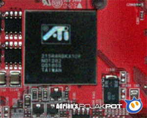
ATI has chosen to use a bridge chip as this card was meant as a native PCIe card.
Bridge chip
Here's a closeup of the bridge chip. This chip modifies the interface to that of an AGP card.We can expect a slight reduction in performance over the native PCIe solution.
Up next is the technology that ATI has implemented into its MVP technology.
ATI's MVP technology
ATI calls its mulli-VPU technology "MVP" which is short for Multi Visual Processing. This is acheived by breaking the screen up through Supertiling. After the screen is cut up, the burden of image processing is then split between the VPUs. It has been rumored that ATI has had the supertiling capability already built into their VPUs since the R3XX VPUs.
There is a lot of unconfirmed rumors floating around and we will follow up once we get more info on that (maybe when we get the dual PCIe MVP samples ;) )
I bet you guys are very interested to see how fast this baby performs eh? Before that, lets get into the testing methodology and the fine print. :p
<<< The X800 Pro Ultra 2X : Previous Page | Next Page : The Test Bed, Testing Methodology, Test Results >>>